

In PCB design, manufacturing, and inspection, copper thickness is a critical parameter. It directly affects current-carrying capacity, heat dissipation, and mechanical strength, and it also influences process selection and cost control. That is why engineers, buyers, and even teams working with a heavy copper PCB manufacturer often ask the same question: how do you calculate PCB copper thickness, and why is it usually specified in ounces rather than directly in microns?
The key to calculating PCB copper thickness is understanding the context. In design, you calculate the required copper thickness based on current demand. In manufacturing and quality control, you often measure or back-calculate the actual thickness. In purchasing, you need to understand unit conversions clearly so you do not misread specifications or supplier quotations. This article breaks down three of the most practical methods and covers the full workflow from design to production and inspection.
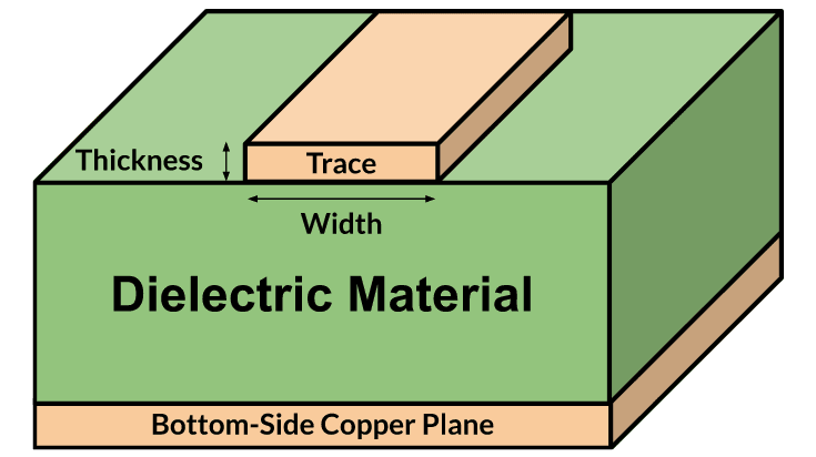
Before getting into the methods, there is one essential point to remember: in the PCB industry, copper thickness is commonly expressed in both weight units and physical thickness units. The most widely used industry approximation is that 1 oz copper corresponds to about 35 μm, which is also about 1.37 mils. Once you remember that conversion, you can solve most copper-thickness questions much more easily.
Basic Knowledge: Understand the Unit Conversions First
Before calculating copper thickness, you need to understand the unit conversions. Otherwise, it is easy to make mistakes by mixing ounces, microns, millimeters, and mils.
The most common units used for PCB copper thickness are ounces (oz), microns (μm), and millimeters (mm). In some cases, mils are also used. The core conversions are:
- 1 oz ≈ 35 μm
- 1 oz ≈ 0.035 mm
- 1 oz ≈ 1.37 mil
- Extended conversions: 0.5 oz ≈ 17.5 μm, 1.5 oz ≈ 52.5 μm, 2 oz ≈ 70 μm, 3 oz ≈ 105 μm
One important detail is that 1 oz = 35 μm is an industry approximation for copper weight converted to thickness. In practice, actual finished copper thickness can vary slightly because manufacturing steps such as plating, etching, and surface preparation affect the final result. This is especially important for outer layers, where the finished copper weight may differ from the starting foil thickness.
The reason the PCB industry still uses ounces is historical and practical. Copper foil was originally specified by weight spread over a fixed area, and that convention remains standard today.
Method 1: Design Selection Calculation
Estimate Copper Thickness from Current Requirements
In PCB design, the main reason for choosing copper thickness is to make sure the trace can safely carry the required current. Thicker copper improves current capacity and thermal performance, but it also increases cost and may affect manufacturability.
For quick estimation, many engineers still use the IPC-2221 empirical formula, although IPC-2152 is generally considered the more accurate standard for trace-current design in modern boards. IPC-2221 remains useful for conservative first-pass sizing.
Simplified IPC-2221 Formula
The common IPC-2221 current-capacity formula is:
I = k ⋅ ΔT⁰.⁴⁴ ⋅ A⁰.⁷²⁵
Where:
- I = maximum current in amperes
- k = correction constant
-
- 0.048 for external layers
- 0.024 for internal layers
- ΔT = allowable temperature rise in °C
- A = conductor cross-sectional area in square mils
Step-by-Step Process
Step 1: Define the design requirements: maximum current, allowable temperature rise, and trace width.
Step 2: Calculate the conductor cross-sectional area:
A=trace width (mil)×copper thickness (mil)
Since 1 oz ≈ 1.37 mil, you can convert copper weight into thickness first.
Step 3: Use the formula to estimate the required cross-sectional area, then back-calculate the copper thickness.
Practical Example
Suppose you are designing a standard consumer-electronics PCB with:
- external trace width = 20 mil
- required current = 2.5 A
- allowable temperature rise = 20°C
Using:
- I=2.5
- ΔT = 20
- k=0.048 for an external layer
you can solve for the required cross-sectional area A, then divide by the trace width to estimate the copper thickness. For a case like this, 1 oz copper is often a reasonable practical choice, which is why 1 oz remains the most common option in many standard electronics products. IPC-2221 is conservative, so in real designs engineers often verify the result with IPC-2152 tools or thermal simulation.
Rule-of-Thumb Values
In everyday design work, engineers often use practical estimates instead of solving the formula every time:
- 1 oz (35 μm): about 1–2 A per 1 mm trace width
- 2 oz (70 μm): about 2–4 A per 1 mm trace width
- 3 oz (105 μm) and above: often used for high-current designs such as power boards, automotive electronics, and other heavy-copper applications
Internal layers dissipate heat less effectively than external layers, so the current capacity is lower for the same copper thickness. That is one reason IPC-2152 is often preferred for more realistic estimates.
Method 2: Manufacturing and Inspection Calculation
Measure or Back-Calculate the Actual Copper Thickness
During PCB production and quality control, the goal is usually to verify whether the finished copper thickness matches the specification. Two common approaches are physical measurement and weight-based back-calculation.
3.1 Physical Measurement Method
Best for Outer-Layer Copper
The most direct approach is to measure the physical thickness of the outer copper using a thickness gauge. In production environments, this is commonly done with non-destructive thickness measurement equipment designed for plated or conductive layers.
A typical workflow is:
- Calibrate the instrument using standard coupons with known copper thickness.
- Select several test points in clean, exposed copper areas.
- Measure multiple points and use the average as the outer-layer copper thickness.
This method is straightforward and fast, but it is generally suitable for surface copper only. It does not directly measure buried inner-layer copper.
3.2 Weight-Based Back-Calculation Method
Better for Total Copper Estimation
The second method uses copper density to back-calculate thickness from mass and area. The corrected formula is:
Copper thickness (μm)=(Weight before etching−Weight after etching/PCB area×Copper density)×104
Where:
- weight is in grams
- area is in cm²
- copper density is 8.96 g/cm³
- the factor 10^4 converts the result from cm to μm
This works because:
g/cm²⋅g/cm³=cm
and then:
1cm=10^4μm
Example
Suppose:
- effective PCB area = 100 cm²
- weight before etching = 25 g
- weight after etching = 23.5 g
Then:
- copper mass = 1.5 g
- thickness:
Copper thickness=(1.5/100×8.96)×10^4≈16.7μm
So the average copper thickness is about 16.7 μm, which is close to 0.5 oz copper. This is consistent with common industry conversions.
For multilayer boards, if you need layer-by-layer verification, cross-section analysis is often more meaningful than a simple total-weight method. The weight method is best used as an average estimate unless the board is specially prepared for layer-specific analysis.
Method 3: Purchasing and Incoming Inspection
Unit Conversion + Spec Verification
When buying PCBs or checking incoming boards, the main task is not complex calculation. It is to verify that the supplier’s copper specification matches your design intent.
What to Check
- Confirm the unit clearly.
If the supplier lists 1 oz, that usually means about 35 μm.
If the supplier lists 2 oz, that usually means about 70 μm. - Clarify whether the spec refers to base copper or finished copper.
This is especially important for outer layers, because base copper plus plating equals finished copper. Some suppliers quote starting foil thickness, while others quote final copper thickness after plating. - Watch for wording such as “1 oz base copper, 1.5 oz finished copper.”
That means the outer layer started with 1 oz foil and gained additional thickness during plating. If you do not clarify this, it is easy to misunderstand the actual finished board capability.
Because acceptance limits vary by fabricator, board class, and drawing requirements, it is better to verify tolerances against the fabrication drawing, purchase specification, or the agreed manufacturing standard rather than assume a single universal percentage for every board.
Common Mistakes Beginners Should Avoid
Mistake 1: Treating “1 oz = 35 μm” as an exact physical constant
In practice, 1 oz copper is commonly treated as about 35 μm, while the exact conversion is slightly lower, around 34.8 μm, and real finished thickness can differ depending on processing. For most design, quoting, and routine inspection work, the 35 μm approximation is perfectly acceptable.
Mistake 2: Ignoring the difference between starting copper and finished copper
This is especially common on outer layers. Finished outer copper includes plating, while inner layers generally do not. If the drawing is unclear, confusion can easily happen between the design team, purchaser, and supplier.
Mistake 3: Assuming a surface thickness gauge can measure inner-layer copper
It usually cannot. Surface measurement methods are mainly for outer copper. Inner copper generally requires destructive cross-sectioning or indirect verification methods.
Mistake 4: Relying only on IPC-2221 for critical high-current design
IPC-2221 remains useful for quick estimates, but IPC-2152 is generally considered more realistic for modern PCB current-carrying calculations because it accounts better for real board conditions.
Conclusion
Calculating PCB copper thickness is not actually complicated once you understand what you are trying to achieve. In design, use practical estimates and current-based calculations to select the right copper weight. In manufacturing and quality control, use measurement or back-calculation to verify the real thickness. In purchasing and incoming inspection, focus on unit conversion and on whether the supplier is quoting base copper or finished copper.
If you remember the core conversion of 1 oz ≈ 35 μm, you can handle most everyday copper-thickness questions with confidence. For most standard PCBs used in consumer electronics or general industrial control, 1 oz copper remains the most cost-effective choice. For higher current and better thermal performance, 2 oz or heavier copper is often preferred. For finer-line designs such as HDI boards, 0.5 oz copper may be the better fit.
If you need more precise results, professional tools can help. Many PCB design platforms and online calculators provide copper-thickness and trace-current estimation features based on IPC models, which can improve both speed and consistency during design validation.
